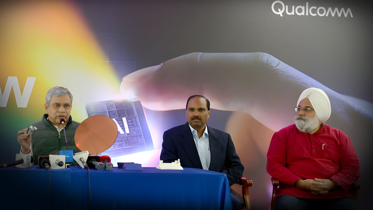
India took a significant step in its semiconductor journey as Union Minister for Electronics and Information Technology Ashwini Vaishnaw unveiled a 2-nanometre (2 nm) chip designed by Qualcomm, underscoring the country’s advancing capabilities in cutting‑edge chip design and the broader ambitions of the newly announced Semicon India 2.0 roadmap.
Why the 2 nm chip matters
The 2 nm architecture represents one of the most advanced process nodes in the semiconductor industry, delivering higher performance and improved energy efficiency compared with earlier generations. At this scale, individual wafers can host tens of billions of transistors in a compact layout, enabling more compute per watt—an advantage for applications ranging from smartphones and data‑centre accelerators to artificial intelligence (AI) workloads.
For India, the reveal is both symbolic and strategic. Semiconductors underpin critical sectors including consumer electronics, electric vehicles, defence systems and telecom infrastructure. Progress in next‑generation chip design strengthens India’s standing in global supply chains and helps reduce long‑term dependence on imports for high‑value technology components.
Qualcomm’s growing footprint in India
Global semiconductor firm Qualcomm has been expanding its design and research presence in India. The 2 nm design announcement highlights that Indian engineering teams are now contributing to sophisticated system‑on‑chip (SoC) development, including integration of advanced CPU and GPU subsystems on a single die.
This engagement signals a shift beyond software and services: India’s talent pool is increasingly active in deep‑tech domains that require specialised expertise, long development cycles and rigorous validation workflows.
Semicon India Mission 2.0: scope and intent
Semicon India 2.0 advances the government’s earlier efforts by pursuing a more comprehensive semiconductor ecosystem. Rather than focusing on a single link in the chain, the new roadmap targets the full value stream—design, fabrication, assembly, testing, packaging and related equipment and materials.
Key policy objectives include nurturing domestic design houses, attracting global fabs and ATMP (assembly, test, mark and pack) facilities, supporting startups and strengthening research collaborations. The programme is oriented toward a multi‑decade horizon to provide policy stability and to encourage capital commitments from both domestic and foreign investors.
Building talent and capability
Human capital is central to the mission. Under the initial phase, the government and academic partners expanded training in chip design, VLSI and related disciplines; thousands of engineers have received hands‑on exposure through updated curricula and advanced design tools.
These initiatives aim to produce professionals capable of end‑to‑end design tasks—tape‑outs, verification, and system validation—thereby raising India’s ability to participate in and lead complex semiconductor projects.
Implications for India’s technology trajectory
The combination of a 2 nm design demonstration and Semicon India 2.0 signals a strategic pivot: India seeks to be recognised not merely as a manufacturing destination but as a hub for advanced technology creation. Growing capabilities in chip design and ecosystem development could enhance strategic resilience, create high‑value jobs, and support emerging sectors such as AI and electric mobility.
Realising these outcomes will depend on sustained policy execution, private‑sector investment, and continued skill development. If these elements align, India’s strengthened role in the global semiconductor landscape could expand significantly over the coming decade.


